

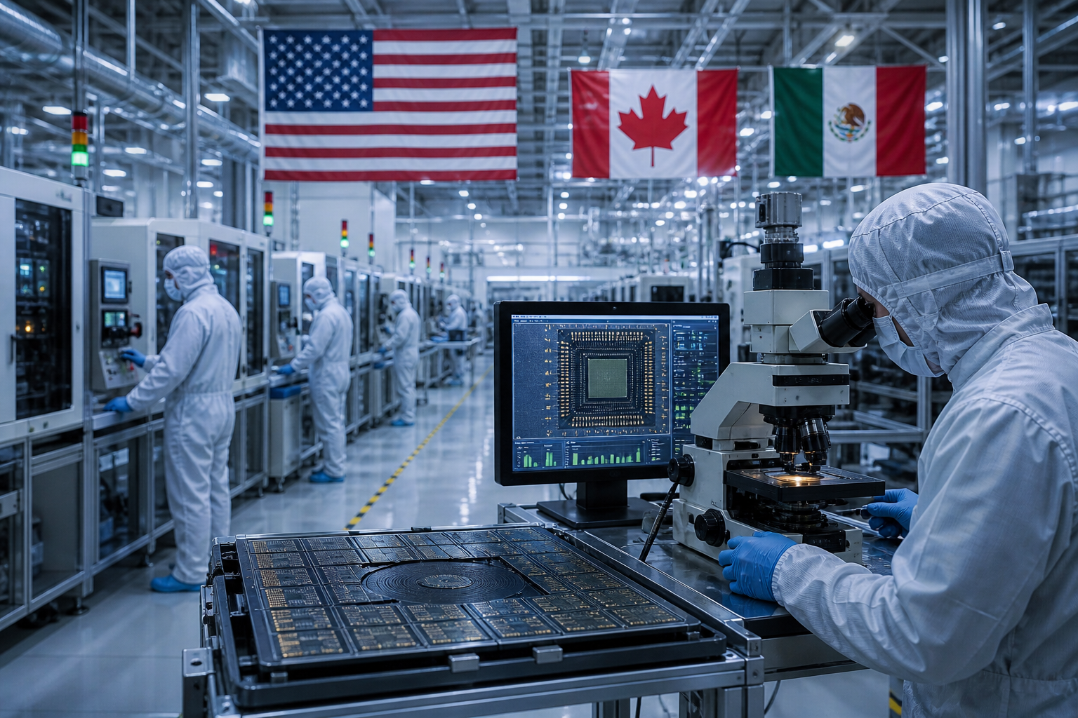
A significant expansion of the technological infrastructure in the United States has been confirmed by Taiwan Semiconductor Manufacturing Co (TSMC), with the announcement of plans to establish an advanced chip packaging facility in Arizona by the year 2029. This strategic initiative, as detailed by senior executive leadership, is intended to address one of the most critical bottlenecks in the global production of modern artificial intelligence hardware. It is maintained that the high-performance chips utilized by industry leaders, such as Nvidia, are no longer characterized as monolithic, single-component entities; rather, they are composed of multiple chips integrated through sophisticated advanced packaging technologies. The current concentration of this specific manufacturing step in East Asia has been identified as a primary constraint for global technology firms, necessitating a geographic redistribution of these essential capabilities.
Earlier in the 2026 fiscal year, it was disclosed that permits were being sought for the commencement of construction within an existing Arizona facility, although a definitive operational timeline had remained unspecified until recently. During a technology conference held in Santa Clara, California, it was formally indicated that construction activities have officially begun. The objective of this development is the aggressive expansion of domestic capabilities, specifically the implementation of CoWoS (Chip on Wafer on Substrate) and 3D-IC (Three-Dimensional Integrated Circuit) packaging technologies. These processes are currently in exceptionally high demand due to their role in enabling the high-speed data transfer required for generative artificial intelligence and high-performance computing applications.
The necessity for such a facility in North America is underscored by the current logistical inefficiencies faced by major technology clients. While companies including Apple and Nvidia have already begun sourcing silicon wafers from existing Arizona fabrication sites, a significant portion of these components must presently be transported back to Taiwan for the final packaging stage. The establishment of localized packaging capacity is therefore viewed as a mechanical requirement for the creation of a fully integrated, domestic end-to-end semiconductor supply chain. By eliminating the need for trans-Pacific transit for final assembly, the resilience of the supply chain against geopolitical instability and logistical disruptions is expected to be substantially enhanced.
The landscape of advanced packaging in Arizona is further complicated by the activities of other industry participants. It has been noted that Amkor Technology previously indicated its intention to establish a similar packaging facility in the region by mid-2027, with production slated to begin by early 2028. This timeline suggests that Amkor may reach operational status significantly earlier than the 2029 goal established by the Taiwanese firm. Although a collaborative agreement was announced between the two entities in 2024 to bring specialized packaging technologies to Arizona, specific details regarding the division of labor and technological exchange have remained undisclosed to the public.
It has been confirmed by Kevin Zhang, the deputy co-chief operations officer and senior vice president at TSMC, that technical discussions with Amkor are currently ongoing. The partnership is being utilized to evaluate the specific technological capabilities that can be offered to shared customers, with the ultimate goal of accelerating the manufacturing of advanced products within the United States. It was remarked that the project still involves several “moving parts,” and a commitment to exploring all possibilities for a diverse manufacturing footprint has been maintained. This flexible approach is intended to allow for the adaptation of the project to evolving market demands and technological shifts within the “Muskonomy” of the mid-2020s, where the speed of innovation often dictates the necessity of local infrastructure.
The strategic significance of this project extends beyond immediate commercial interests. The localization of advanced packaging is interpreted as a critical component of national economic security, ensuring that the most sophisticated hardware required for defense, telecommunications, and industrial automation can be produced within a secure jurisdiction. As the global semiconductor industry transitions toward a more fragmented and regionalized model, the successful execution of the Arizona packaging plant will serve as a benchmark for future international investments.
Ultimately, the commitment to bring 3D-IC and CoWoS capabilities to Arizona by 2029 represents a long-term investment in the technological sovereignty of the North American market. While the 2029 deadline is viewed by some as distant compared to competitor timelines, the scale and technical complexity of the endeavor are cited as justifications for the rigorous developmental schedule. The transition from a centralized manufacturing model to a distributed global network is being managed with meticulous oversight, ensuring that the next generation of artificial intelligence hardware is supported by a robust and geographically diverse physical infrastructure. As construction continues, the focus of the industry will remain on the integration of these localized facilities into the broader global silicon ecosystem, providing the stability and scale required for the continued advancement of the digital age.